APPLIED PHYSICS LETTERS 95, 123107 ͑2009͒
1
1
1,3
V. Iancu, P. R. C. Kent,
C. G. Zeng, and H. H. Weitering
1
Department of Physics and Astronomy, The University of Tennessee, Knoxville, Tennessee 37931, USA
Center for Nanophase Materials Sciences, Oak Ridge National Laboratory, Oak Ridge,
2
Tennessee 37831, USA
3
Materials Science & Technology Division, Oak Ridge National Laboratory, Oak Ridge,
Tennessee 37831, USA
͑
Received 13 May 2009; accepted 3 September 2009; published online 23 September 2009͒
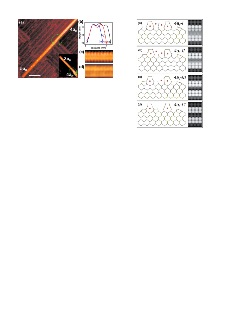
Exceptionally long and uniform YSi nanowires are formed via self-assembly on Si͑001͒. The
2
in-plane width of the thinnest wires is known to be quantized in odd multiples of the silicon lattice
constant. Here, we identify a class of nanowires that violates the “odd multiple” rule. The structure
of the thinnest wire in this category is determined by comparing scanning tunneling spectroscopy
measurements with the calculated surface density of states of candidate models by means of the
Individual nanometer-sized objects have been the focus
of many experimental and theoretical studies in recent years
because of their special appeal to fundamental science and
because of their interesting chemical and physical properties
far too low for structure determination via surface x-ray dif-
fraction or low energy electron diffraction ͑LEED͒. There-
fore, scanning tunneling microscopy ͑STM͒ remains the
most powerful tool for in situ investigation of their structure
and electronic properties. However, STM images contain
that may one day find their use in nanotechnology. Metal-
lic nanowires embedded in a Si platform are particularly
interesting because they might be used as metallic intercon-
both topographical and electronic structure information and
therefore the image interpretation necessarily relies on sup-
porting electronic structure calculations and theoretical im-
age simulations, for a given structure model. In the present
nects in Si-based nanodevices.
For this matter, it is cru-
cially important to elucidate their structural and electronic
properties.
case of YSi , the competing models of the nanowires pro-
2
Epitaxial YSi nanowires represent an interesting case in
duce theoretical STM images that are qualitatively very simi-
lar. To determine the most likely structure, we introduce a
reliability factor or R factor to quantify the agreement be-
tween the normalized dI/dV spectra from STS and the den-
sity functional theory ͑DFT͒ calculated surface projected
density of states ͑PDOS͒, and apply this method to determine
the structure of the 4a YSi nanowires.
2
point. These nanowires are formed via self-assembly after
depositing approximately 0.5 ML ͑monolayer͒ of Y onto
an atomically clean Si͑001͒ surface in ultrahigh vacuum
͑
UHV͒. Most of the Y is incorporated into a ͑2ϫ7͒ wetting
on top. The wires have extraordinary aspect ratios and can
grow up to microns long. The reported cross sections of the
0
2
Experiments were performed in a UHV system with a
base pressure of 1ϫ10− mbar. Y was deposited through
e-beam evaporation onto an atomically clean Si͑001͒2ϫ1
substrate held at 625Ϯ25 °C. All STM/STS measurements
were carried out using an Omicron VT-STM operated at
room temperature. Spectroscopy was performed by recording
the tunneling current ͑I͒ while ramping the tunneling bias
2
10
thinnest wires are 0.4ma nm , where m represents an odd
0
integer ͑m=3,5,7,9͒ and a =0.384 nm the lattice constant
0
of the Si͑001͒ plane. We refer to these nanowires in terms of
their width, i.e., 3a for 1.15 nm wide and 5a for 1.92 nm
0
0
wide wires. Although many metals can be used to create
silicide nanowires, YSi wires have the highest aspect ra-
2
tio so far, probably because of the large anisotropic mismatch
͑
V͒ at specific locations on the nanowires. The differential
between the silicides AlB structure and Si substrate and the
2
conductance ͑dI/dV͒ was obtained by numerical differentia-
tion of the I-V curves and subsequent normalization to the
I/V ratio to remove the contribution of the transmission
¯
near-perfect lattice match along the Si direction ͓110͔.
In this letter, we report on the existence of YSi nano-
2
wires that violate the odd-multiple rule for stable wire
widths. We investigate the structure and electronic properties
of the thinnest nanowire in the even-multiple category by
adopting a reliability or R-factor analysis for comparing
scanning tunneling spectroscopy ͑STS͒ data with first-
function.
To assess the possible YSi nanowires structures, we
2
performed total energy calculations. We used DFT, imple-
method
and the local density approximation. We used
principles calculations. The formation enthalpies of the 3a ,
0
supercells containing a slab with nine layers of Si atoms.
Hydrogen atoms passivated the rear surface. The bottom two
layers of atoms were held fixed at the theoretical bulk lattice
positions. All other atoms were allowed to fully relax. Super-
4
a , and 5a wires are also computed.
0
0
These extremely thin nanowires are too small and fragile
to be subjected to ex situ sample processing for, e.g., trans-
mission electron microscopy, while their number density is
cell dimensions were up to 16ϫ2ϫ8.48a , containing up to
0
3
78 atoms. The 16a width allows for the study of relatively
0
a͒Electronic mail: kentpr@ornl.gov.
isolated nanowires. We used the same basis set and conver-
0
003-6951/2009/95͑12͒/123107/3/$25.00
95, 123107-1
36.165.238.131 On: Mon, 22 Dec 2014 19:48:39
© 2009 American Institute of Physics
This article is copyrighted as indicated in the article. Reuse of AIP content is subject to the terms at: http://scitation.aip.org/termsconditions. Downloaded to IP:
1

 Iancu
Iancu