C404
Journal of The Electrochemical Society, 151 ͑6͒ C399-C404 ͑2004͒
rate can be estimated at 5 ϫ 10Ϫ4 Ϫ 5 ϫ 10Ϫ2 ML/s at 685-790 K
at the full H coverage for both ͑100͒ and ͑111͒ surfaces. On the
Acknowledgments
The authors thank Professor Fumio Okada for his helpful discus-
sion and comments. This study was partially supported by the In-
dustrial Technology Research Grant Program, 00B64024c, of the
New Energy and Industrial Technology Development Organization
of Japan, and by the Grant-in-Aid for Scientific Research ͑A͒,
15206086, 2003, of the Ministry of Education, Culture, Sports, Sci-
ence and Technology, Japan.
other hand, the reaction rate was 0.18 р R р 1.4 nm/s, which cor-
s
responds to several ML/s. The small desorption rate of H implies
2
that the H desorption is the rate-determining step, however, it is too
2
small to account for the observed reaction rate. One possible reason
is the difference in the Si surface structure. The surface was atomi-
cally smooth in Ref. 17 and 18, whereas it was rough in this work.
As for the activation energy, it was 190-250 kJ/mol for H desorp-
2
The University of Tokyo assisted in meeting the publication costs of this
article.
tion in Ref. 17 and 18, whereas it was about 60 kJ/mol for R in Fig.
s
9. This large difference in activation energy might also be caused by
the difference in the Si surface structure, but we lack information to
determine which is the rate-determining step, Reactions 13 or 14.
List of Symbols
The mechanism of H desorption is still unclear, even for the atomi-
2
19
cally smooth surfaces of monocrystalline Si.
CHCl HCl concentration, vol %
cHCl
HCl concentration, mol/m
We summarize the overall production rate of SiHCl below. The
3
3
3
reaction rate per unit reactor volume, Rtotal (mol/m /s), can be ex-
cr conversion ratio of Si particles
pressed as
crf final conversion ratio in the model
f
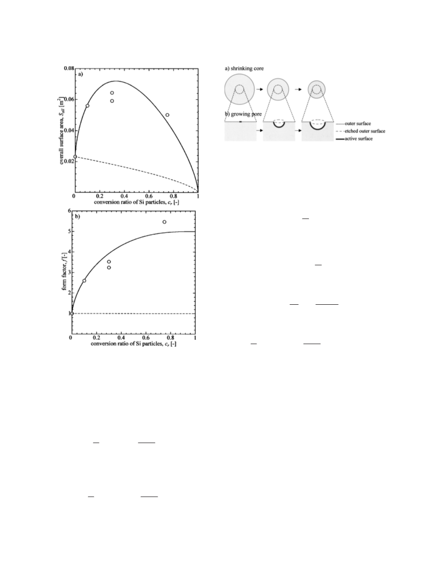
ratio of actual surface area of Si particles to that calculated by using the
shrinking-core model
SV
Rtotal
ϭ
Rs
͓15͔
f
Ј
ratio of generated area of the activated surface to area of inactive surface
lost
M
k
reaction rate constant, m2.5/mol0.5/s
atomic weight of Si, kg/mol
3
3
where ϭ 2.33 ϫ 10 (kg/m ) is the density of crystalline Si,
M
N
P
2
3
number of active points on each Si particle
gas pressure, Pa
SV (m /m ) is the activated surface area of Si per unit reactor vol-
Ϫ3
ume, and M ϭ 28.09 ϫ 10 (kg/mol) is the atomic weight of Si.
The reaction rate used in the model of Fig. 9 was
Q
R
total flow rate of reactant gases, sccm
gas constant, J/mol/K
Rs reaction rate of activated Si surfaces, m/s
Rtotal reaction rate per unit reactor volume, mol/m /s
0
.5
R ϭ kc
͓16͔
3
s
HCI
2
S
S0
outer surface area of Si particles, m
initial surface area of Si particles, m
where cHCl (mol/m ) is the HCl concentration and k ͑m2.5/mol0.5/s͒
3
2
2
Sa area of activated surface of Si particles, m
is a rate constant expressed as
Sall overall surface area of reacted Si particles, m2
Se area of etched outer surface of Si particles, m
SV activated surface area of Si particles per unit reactor volume, m /m
2
6
0͑kJ/mol͒
k ϭ 2.5 ϫ 10Ϫ5͑m2.5/mol0.5/s͒exp
Ϫ
͓17͔
2
3
ͫ
ͬ
RT
t(s), t ͑min͒
reaction time
T
V
temperature, K
the volume of the reacted Si particles, m
3
where R ϭ 8.314 (J/mol/K) is the gas constant. These equations
can be used to estimate the production rate of SiHCl at 623 р T
р 723 K and 0.15 р cHCl р 1.8 mol/m .
3
V0 the volume of the unreacted Si particles, m
3
density of crystalline Si, kg/m
3
3
References
Conclusions
1
. R. Brendel, Jpn. J. Appl. Phys., Part 1, 40, 4431 ͑2001͒.
With the objective of designing a CVD process with closed gas
recycling for making low-cost, crystalline silicon thin films for solar
cells, we studied the formation of chlorosilanes by the reaction of Si
with HCl. The reaction rate was time dependent and did not corre-
late well with reaction time, but correlated well with the conversion
ratio of Si. Many pores were formed on the surface of particles
during the reaction, these pores acted as active sites, and the reaction
rate increased with increasing pore area. Pretreatment by fluidizing
2. S. Noda, K. Hagiwara, O. Ichikawa, K. Tanabe, T. Yahiro, H. Ohkawa, T. Osawa,
and H. Komiyama, in Proceedings of 29th IEEE Photovoltaic Specialists Confer-
ence, New Orleans, 308 ͑2002͒.
3
4
. I. Shiihara and J. Iyoda, Bull. Chem. Soc. Jpn., 32, 636 ͑1959͒.
. G. A. Lang and T. Stavish, RCA Rev., 24, 488 ͑1963͒.
5. L. V. Gregor, P. Balk, and F. J. Campagna, IBM J. Res. Dev., 9, 327 ͑1965͒.
6. Th. J. M. Kuijer, L. J. Giling, and J. Bloem, J. Cryst. Growth, 22, 29 ͑1974͒.
7. P. van der Putte, L. J. Giling, and J. Bloem, J. Cryst. Growth, 41, 133 ͑1977͒.
8. J. Bloem and W. A. P. Claassen, J. Cryst. Growth, 49, 435 ͑1980͒.
9. C. Dominguez, G. Pastor, and E. Dominguez, J. Electrochem. Soc., 134, 200
͑1987͒.
the particles with an H stream for 120 min at T ϭ 773 K signifi-
2
1
0. C. Dominguez, G. Pastor, and E. Dominguez, J. Electrochem. Soc., 134, 202
1987͒.
1. H. Habuka, H. Tsunoda, and T. Otsuka, J. Electrochem. Soc., 145, 4264 ͑1998͒.
2. J. Y. P. Mui, Corrosion (Houston), 41, 63 ͑1985͒.
13. Y. Ohshita and N. Hosoi, Appl. Phys. Lett., 63, 1216 ͑1993͒.
cantly decreased the incubation time before the reaction started,
causing the time profile of the reaction rate to become repeatable.
We developed a reaction model called the shrinking-core model with
growing pores, and successfully correlated the time-dependent reac-
tion rates with the surface-area change for 623 р T р 723 K and
for 1.0 р CHCl р 10 vol%. By using this model, reaction rates per
unit area of activated surfaces were estimated and expressed in the
form of a rate equation that can be used to design CVD reactors. To
realize low-cost production of solar cells, it is important not only to
couple the reaction kinetics of chlorosilane synthesis and Si-CVD
͑
1
1
1
1
4. S. Bade, U. Hoffmann, and K. Schonert, Int. J. Min. Process., 44-45, 167 ͑1996͒.
5. A. P. Belyi, A. I. Gorbunov, R. M. Flid, S. A. Golubtsov, N. S. Feldshtein, and I. V.
Trofimova, Coll. Czech. Chem. Conn., 32, 1359 ͑1967͒.
16. A. P. Belyi, A. I. Gorbunov, R. M. Flid, and S. A. Golubtsov, Russ. J. Phys. Chem.,
43, 637 ͑1969͒.
7. K. Subbuag, M. G. Sherman, L. B. Kewis, W. H. Weinberg, J. T. Yates, Jr., and K.
C. Janda, J. Chem. Phys., 92, 5700 ͑1990͒.
8. M. L. Wise, B. G. Koehler, P. Gupta, P. A. Coon, and S. M. George, Surf. Sci., 258,
1
1
2
but also to couple the CVD process with closed gas recycling with
1
66 ͑1991͒.
1
the layer transfer processes for Si thin-film production.
19. W. Brenig, H. J. Kreuzer, and S. H. Payne, Phys. Rev. B, 67, 205419 ͑2003͒.

 Noda, Suguru